
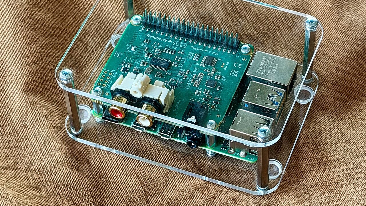
An Inter-IC Sound (I2S) digital audio interface is a synchronous three-wire serial bus standardized by Philips Semiconductors (now NXP Semiconductors) specifically for streaming uncompressed digital audio between integrated circuits on a printed circuit board. Instead of mixing configuration commands with audio data or routing noise-prone analog traces across a board, I2S separates clock timing and pulse-code modulation (PCM) audio samples onto dedicated pins: a continuous serial bit clock, a word select line, and a serial data line. On microcontrollers, the I2S peripheral pairs directly with Direct Memory Access (DMA) hardware so stereo audio buffers move continuously between memory and external amplifiers, codecs, or microphones without requiring the processor to handle individual samples.
Why do microcontrollers use I2S instead of SPI or I2C for audio?
Philips Semiconductors originally introduced the I2S specification in February 1986, revised it in June 1996, and updated it in February 2022 as NXP User Manual UM11732 (Revision 3.0). The specification defines a board-level link strictly for transferring digital audio samples between integrated circuits such as analog-to-digital converters (ADCs), digital-to-analog converters (DACs), digital signal processors, and microcontrollers.
General-purpose buses serve different needs on a circuit board. Inter-Integrated Circuit (I2C) is a two-wire control bus built for addressing registers and reading low-speed sensors, while Serial Peripheral Interface (SPI) transfers general data packets using chip-select lines. In an audio design, an engineer typically uses I2C or SPI to configure an external codec’s volume registers or power states, while reserving the I2S bus solely for the continuous audio stream.
Keeping clock signals on dedicated lines separate from the serial data wire avoids the complex clock-recovery circuitry required by single-wire asynchronous interfaces. It also minimizes timing jitter that would otherwise distort analog reconstruction inside a DAC or corrupt sampling inside an ADC.
What do the I2S clock and data pins do?
The February 2022 NXP specification uses the terms controller and target in place of the older master and slave terminology. Whichever chip drives the bus clocks acts as the controller, and chipmakers often print slightly different pin labels on their datasheets for the same three core wires plus an optional fourth clock.
- Continuous Serial Clock (SCK), commonly labeled Bit Clock (BCLK), carries one clock pulse for every digital audio bit transmitted across the bus. You calculate its frequency by multiplying the audio sampling rate by the number of bits per channel slot and the number of channels.
- Word Select (WS), also labeled Left/Right Clock (LRCLK), Word Clock (WCLK), or Frame Sync (FS), runs at a frequency equal to the audio sampling rate. In standard Philips mode, a low logic level (WS = 0) indicates that Channel 1 (left) is being transmitted, and a high logic level (WS = 1) indicates Channel 2 (right).
- Serial Data (SD), often labeled SDATA, SDIN, SDOUT, DIN, or DOUT, carries the left and right audio words multiplexed in time over a single wire. Samples are encoded in signed two’s complement format with the Most Significant Bit (MSB) transmitted first.
- Master Clock (MCLK) is an optional fourth signal that is not part of the base three-wire NXP specification. Microcontrollers frequently output MCLK at a fixed multiple of the sampling rate, such as 256 times the sample frequency, to drive the internal delta-sigma modulators and digital oversampling filters inside external audio codecs.
Because a single Serial Data line only travels in one direction, streaming microphone audio into a microcontroller while simultaneously playing audio out to an amplifier requires two data pins (DIN and DOUT). Full-duplex controllers, such as those documented in the Espressif ESP-IDF I2S reference (2026), share a single pair of BCLK and WS clock lines across both data pins at the same time.
How does the I2S one-bit delay handle different bit depths?
If you inspect a standard Philips I2S bus on an oscilloscope or logic analyzer, you will notice that a new audio word does not start on the exact clock edge where the Word Select line flips from left to right. Instead, the MSB of the new word is transmitted one SCK clock period after the WS transition. Transmitters typically change the states of both WS and SD on the trailing (falling) edge of SCK, while the receiver latches the incoming data bit on the leading (rising) edge.
That one-clock delay gives a target transmitter time to derive synchronous timing from the WS edge and gives a receiver one clock cycle to store the completed previous word and prepare its shift register for the incoming channel. In NXP’s timing specifications for a 2.5 MHz target receiver (minimum clock period of 360 nanoseconds), the clock high and low phases must each last at least 110 nanoseconds, with a minimum data setup time of 60 nanoseconds before the rising clock edge.
Sending the MSB first at a fixed position one clock cycle after the WS transition also solves word-length mismatches automatically. Neither the transmitter nor the receiver needs to know how many bits the other chip supports:
- When a 24-bit digital MEMS microphone streams samples into a microcontroller configured for 16-bit channel slots, the microcontroller latches the first 16 bits after the WS transition and ignores the remaining 8 Least Significant Bits (LSBs).
- When a microcontroller transmits 16-bit samples inside a 32-bit frame to a 24-bit DAC, the DAC loads the 16 incoming bits into its upper bit positions and pads the remaining lower bits with zeros.
For multi-channel hardware that needs more than left and right stereo on a single data wire, engineers switch the interface from two-channel I2S to Time-Division Multiplexing (TDM). As outlined in Analog Devices technical article MS-2275 (2012), TDM divides each frame sync period into four, eight, or sixteen consecutive channel slots while running the bit clock proportionally faster.
How do microcontrollers stream I2S audio using DMA and audio clocks?
Streaming uncompressed stereo audio requires continuous, deterministic timing. According to Analog Devices (2012) and STMicroelectronics Application Note AN4309 (2014), playing 48 kHz stereo audio across 32-bit channel slots requires a bit clock of 3.072 MHz (48,000 Hz multiplied by 32 bits multiplied by 2 channels). When an external codec also requires a 256x Master Clock, the microcontroller outputs a 12.288 MHz signal on its MCLK pin.
If a microcontroller CPU had to load a register via software interrupt three million times a second, it would have no cycles left to decode audio files, draw a display, or manage wireless network traffic. Instead, microcontroller I2S peripherals feed small hardware First-In, First-Out (FIFO) buffers connected to a Direct Memory Access (DMA) controller. You pass the DMA controller a pointer to an audio buffer in RAM, and the DMA hardware automatically pushes words into the I2S shift register whenever space opens in the FIFO, firing a CPU interrupt only when an entire buffer block finishes playing.
Hardware layout varies across microcontroller families:
- On STMicroelectronics STM32L1xx and STM32F103xx microcontrollers, the I2S logic shares hardware pins and registers with the SPI peripheral. Software selects between SPI mode and I2S mode, which operates in simplex (transmit-only or receive-only per peripheral block) and supports Philips I2S, MSB-justified, LSB-justified, and PCM standards using a 9-bit linear divider and an odd-bit prescaler (STMicroelectronics, 2014).
- On Espressif chips, the ESP32 and ESP32-S3 include two independent I2S controllers, while the ESP32-P4 includes three. According to Espressif’s 2026 documentation, these controllers support Standard, Pulse-Density Modulation (PDM), and TDM modes, and can derive their timing from a dedicated Audio Phase-Locked Loop (`I2S_CLK_SRC_APLL`) so standard sample rates like 44.1 kHz or 48 kHz do not suffer division rounding errors from the main system crystal. Projects such as an open-source ESP32-S3 world map radio rely on this background DMA streaming to play internet audio streams smoothly while driving a touchscreen interface.
- On Infineon PSoC architectures, the I2S component supports 8-bit to 32-bit sample depths with configurable 16-, 32-, 48-, or 64-bit word select periods, reaching stereo sample rates up to 96 kHz at a 6.144 MHz bit clock (Infineon Technologies, 2015).
What are the most common I2S configuration mistakes?
Even with only three or four wires to connect, small mismatches between a microcontroller’s firmware configuration and an external audio chip’s datasheet can cause silent outputs, loud static, or periodic clicks.
- Mixing up Philips I2S and Left-Justified (MSB-justified) modes: Both formats send the Most Significant Bit first, which makes them easy to confuse in firmware menus. In standard Philips I2S, the MSB is delayed by one BCLK cycle after WS changes and WS = 0 selects the left channel. In MSB-justified mode, the MSB is output immediately on the exact clock edge where WS changes, with no one-bit delay (STMicroelectronics, 2014). If one chip uses Philips timing and the other uses MSB-justified timing, every audio sample shifts by one bit, doubling or halving the amplitude and corrupting the sign bit.
- Assuming the audio transmitter is always the clock controller: While a microcontroller sending music to an amplifier normally generates BCLK and WS, NXP’s specification allows either the transmitter, the receiver, or a separate third clock generator IC to act as the bus controller. High-precision audio codecs often act as the clock controller using their own low-jitter crystal oscillator, while the microcontroller transmits audio data as a target device synchronized to the codec’s incoming clocks.
- Running MCLK and WS from unlocked clock sources: As documented in Texas Instruments Application Report SLAA469A (2019), delta-sigma ADCs and DACs require their internal master clock to remain frequency-locked to the frame clock (WS). If you feed a codec’s MCLK pin from a standalone crystal oscillator while the microcontroller generates BCLK and WS from its own internal clock divider, tiny frequency drift between the two oscillators will cause the converter to periodically skip or repeat audio samples.
- Wiring MCLK when a target chip does not need it (or omitting it when required): Many standalone two-chip MEMS microphones and class-D smart amplifiers contain an internal phase-locked loop that derives all modulator timing directly from the BCLK pin, leaving no MCLK pin to wire. Conversely, traditional multi-function audio codecs frequently mute their outputs if a synchronized MCLK signal is missing and their internal PLL is not explicitly configured in registers to lock onto BCLK (Analog Devices, 2012; Texas Instruments, 2019).
Frequently asked questions
How do you calculate the I2S bit clock frequency for CD-quality audio?
Multiply the 44,100 Hz sampling rate by 16 bits per channel and 2 stereo channels (`44,100 x 16 x 2`), which equals a continuous bit clock (BCLK) of 1.4112 MHz. If you frame those 16-bit samples inside 32-bit channel slots, the bit clock doubles to 2.8224 MHz.
Can two I2S microphones share the same data wire?
Yes. Because a single microphone only outputs mono audio during half of the Word Select period, you can wire two digital I2S microphones to the exact same BCLK, WS, and SD pins on a microcontroller. By strapping one microphone’s L/R select pin to ground (left, WS = 0) and the other microphone’s select pin to power (right, WS = 1), each microphone drives the data line during its assigned half-frame and places its output in a high-impedance state while the other transmits.