
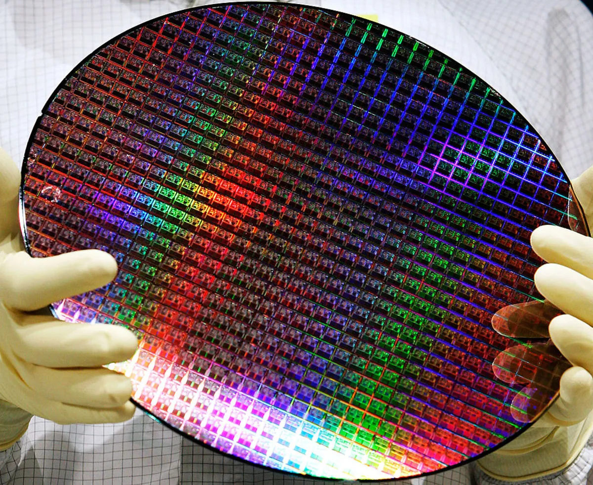
The Core Mechanics: What is a Nanometer?
A nanometer (nm) in computer processors currently functions as a commercial marketing term used by chipmakers to denote a new device generation, rather than a literal physical measurement.
To understand the scale, you must look at the basic mathematics. A nanometer is a metric unit of length equal to one-billionth of a meter. To put this microscopic size into a physical perspective, a single human hair measures roughly 80,000 to 100,000 nanometers wide. Your fingernail grows about one nanometer every second.
Traditionally, the nanometer label on a computer processor referred to an actual physical dimension on the chip. Specifically, it denoted the gate length, which is the physical distance between a transistor’s source and drain. In other cases, it measured half of the metal pitch. These microscopic transistors operate as tiny electrical switches that process binary code.
Reducing the distance between these transistors drives the entire semiconductor industry. When engineers shrink the physical distance between gates, electrons have less physical space to travel. This shorter travel distance means electrical signals move faster across the chip.
Shrinking these components also alters the electrical properties of the processor. Switching states on smaller transistors uses less power because of lower capacitance. This reduced power consumption naturally means less heat is dissipated into the computer system. Manufacturers use the space saved by shrinking these switches to pack billions of additional parallel processing units into the exact same physical footprint. Extra space allows hardware designers to add dedicated GPU shaders or specialized AI engines directly onto the main die.
The Great Shift: Marketing Labels vs. Physical Reality
The naming convention for processor hardware changed permanently around 2011. The nanometer label began to deviate entirely from the actual physical length of the transistor features. Today, a processor labeled as “3 nm” or “5 nm” does not mean any specific physical component inside the chip is literally three or five nanometers in size.
The nanometer number functions purely as a generational shorthand. Companies like TSMC, Intel, and Samsung use these numbers to indicate a new manufacturing process. A smaller number guarantees buyers higher transistor density than the previous generation. It also typically guarantees upgraded transistor geometry. Manufacturers use three-dimensional transistor designs like FinFET (Fin Field-Effect Transistor) or GAAFET (Gate-All-Around Field-Effect Transistor) to manage electron flow. The smaller nanometer label simply promises these better geometries and higher power efficiency.
Engineers use a different metric to measure actual physical density. The International Roadmap for Devices and Systems (IRDS) uses “Contacted Gate Pitch” (CGP). This metric measures the actual physical distance between the gates on the silicon. For example, a modern chip sold under the “5 nm node” label actually has a physical gate length closer to 18 nanometers. The contacted gate pitch for that same processor sits at around 51 nanometers.
This discrepancy explains why different manufacturers with the same “nanometer” label often produce chips with vastly different actual performance metrics. The label is a marketing category, while the CGP dictates the physical density.
Feature Comparison: The Node Shrink Timeline
The history of semiconductor manufacturing shows exactly when the physical measurements decoupled from the marketing names. Here is a breakdown of the distinct processor generations.
- 2003 (The 90 nm Era): In the early 2000s, labels were still highly literal. According to an educational guide by Lam Research, the 90 nm node roughly matched a real metal line half-pitch size of exactly 90 nanometers. If a consumer bought a 90 nm chip, they were buying silicon with features actually measuring 90 nanometers across.
- 2020 (The 5 nm Era): Foundries like TSMC and Samsung entered volume production of 5 nm chips for major consumer tech companies like Apple, Qualcomm, and Huawei. As detailed on the 5 nm process Wikipedia page, this generation offered immense gains. TSMC reported their 5 nm process offered 1.8 times the density of their previous 7 nm process. This density increase resulted in a 15% speed improvement or a 30% reduction in power consumption, despite the physical features not actually measuring five nanometers.
- The 1 nm Horizon (2026 and beyond): The industry is currently targeting the 1 nm process. The IRDS projects that a future 1 nm node will still require a physical Contacted Gate Pitch scaling to about 40 to 42 nanometers. Experimental designs achieve this density in isolated labs. A 2024 report by researchers at Nanjing University utilized semi-metal antimony to achieve a 40 nm CGP, moving away from traditional silicon channels.
Physics Limits and the End of Moore’s Law
The push for smaller nanometer nodes traces its origins back to 1965. Intel co-founder Gordon Moore coined a principle that shaped decades of hardware development. As explained in a history of Moore’s Law, the rule predicted that the number of transistors on a microchip would double roughly every two years. This doubling effect halved the cost of computers while simultaneously doubling their processing power.
Manufacturers are now hitting the hard limits of atomic physics. As transistor gates shrink to just a few atoms thick, typically below the literal 10 nanometer physical mark, electrons behave unpredictably. They begin to leak through the physical barriers via a quantum mechanics phenomenon called quantum tunneling. This leakage ruins the processor’s ability to reliably switch between binary states.
Packing billions of active switches into a tiny area creates massive heat density problems. Cooling these microscopic components requires advanced thermal management systems to prevent the silicon from degrading under its own operating temperatures.
The financial cost of shrinking transistors is equally restrictive. Continuing to push past current density limits requires Extreme Ultraviolet (EUV) lithography machines. These highly specialized manufacturing tools cost upwards of $150 million each. The sheer capital required limits advanced semiconductor manufacturing to just a few global companies.
Industry experts argue the original cadence of hardware improvement is already over. According to MIT Professor Charles Leiserson, the traditional standard of halving sizes every two years broke down around 2016. He points out it took Intel five full years to jump from their 14 nm process to their 10 nm process.
Future performance gains must come from different engineering methods. Researchers emphasize improvements will come from the “top” of the computing stack. This means hardware designers will rely on smarter software algorithms and 3D chip integration. Engineers are stacking processors vertically rather than just packing them tighter horizontally. As shown in ongoing research into the 1 nm process, the industry is also testing alternative materials like graphene, photonics, and carbon nanotubes to eventually replace standard silicon.
Frequently Asked Questions
Is a 3nm processor literally 3 nanometers in size?
No. In modern computer hardware, labels like 3nm or 5nm are generational marketing terms. They indicate a new, more advanced manufacturing process with higher transistor density and efficiency. They do not correspond to the actual physical measurement of the chip’s transistors. The physical gates are significantly larger than the marketing number suggests.
Why do smaller nanometer processors perform better?
Smaller processing nodes allow electrons to travel shorter physical distances. This speeds up signal processing across the chip. Tighter nodes also reduce capacitance, meaning less energy is required to switch the transistors on and off. This efficiency directly results in lower power consumption and reduced heat generation. The space saved by shrinking components allows chipmakers to add more parallel cores to the processor die.
What happens when processors reach 1nm?
Shrinking processor nodes down to 1nm pushes the absolute limits of silicon physics. At these microscopic sizes, electrons start leaking through physical barriers due to quantum tunneling. To bypass these hard physical limits, the semiconductor industry is researching deep architectural changes, such as 3D stacking of chips. They are also testing alternative channel materials like carbon nanotubes and graphene to continue improving processing power without solely relying on traditional silicon node shrinking.